
Size and weight
Multi-element assemblies burden airborne, autonomous, wearable, robotic, and distributed sensing platforms.
Platform
Coherent Photonics develops compact, scalable metasurface components and sensors supported by physics-informed design, fabrication-aware optimization, and internal prototype characterization.
The optical system constraint
Sensing and imaging systems often depend on multiple refractive lenses, mirrors, spacers, mechanical housings, precision alignment steps, and relatively large detector areas.
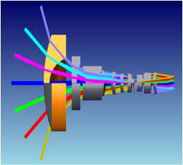
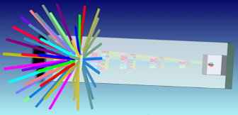
Multi-element assemblies burden airborne, autonomous, wearable, robotic, and distributed sensing platforms.
Precision assembly and tight mechanical tolerances increase cost and integration effort.
Vibration, shock, thermal drift, and mechanical changes can degrade system performance.
Complex assemblies are difficult to translate into resilient, wafer-compatible production.
Small changes in surface shape may result in significant wavefront errors.
Product variants may require custom components and renewed mechanical integration.
Protected intellectual property
Our intellectual property spans the core design methods, optical architectures, and compact components needed to move from beam control to sensing and imaging systems. Together, these areas support multiple applications from a common foundation in sub-wavelength photonics.
Beam control
Compact meta-optic structures for shaping, steering, and combining optical beams without the complexity of conventional multi-element assemblies.
Sensing & illumination
Integrated optical components that support tailored illumination, multi-beam sensing, and compact system architectures.
System architecture
New optical configurations for sensing, imaging, and high-power applications across demanding size, field-of-view, and performance requirements.
Design methods
Physics-informed approaches for designing engineered nano-structures and controlling the optical field at sub-wavelength scales.
Capabilities
Five issued U.S. patents, 12 foundational U.S. patent applications and internal know-how.
Computationally efficient, physics-informed AI/ML optimization with design-for-manufacturing.
Internal nanophotonic performance testing and prototype characterization capability.
Device layouts are developed for process runs with established nanophotonics fabricators.